
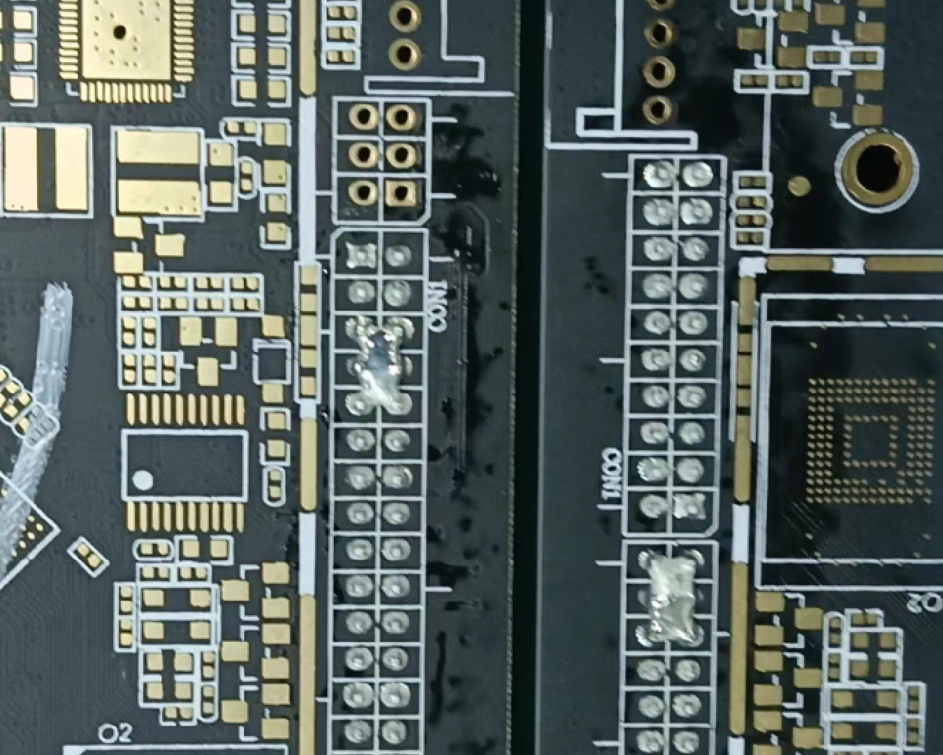
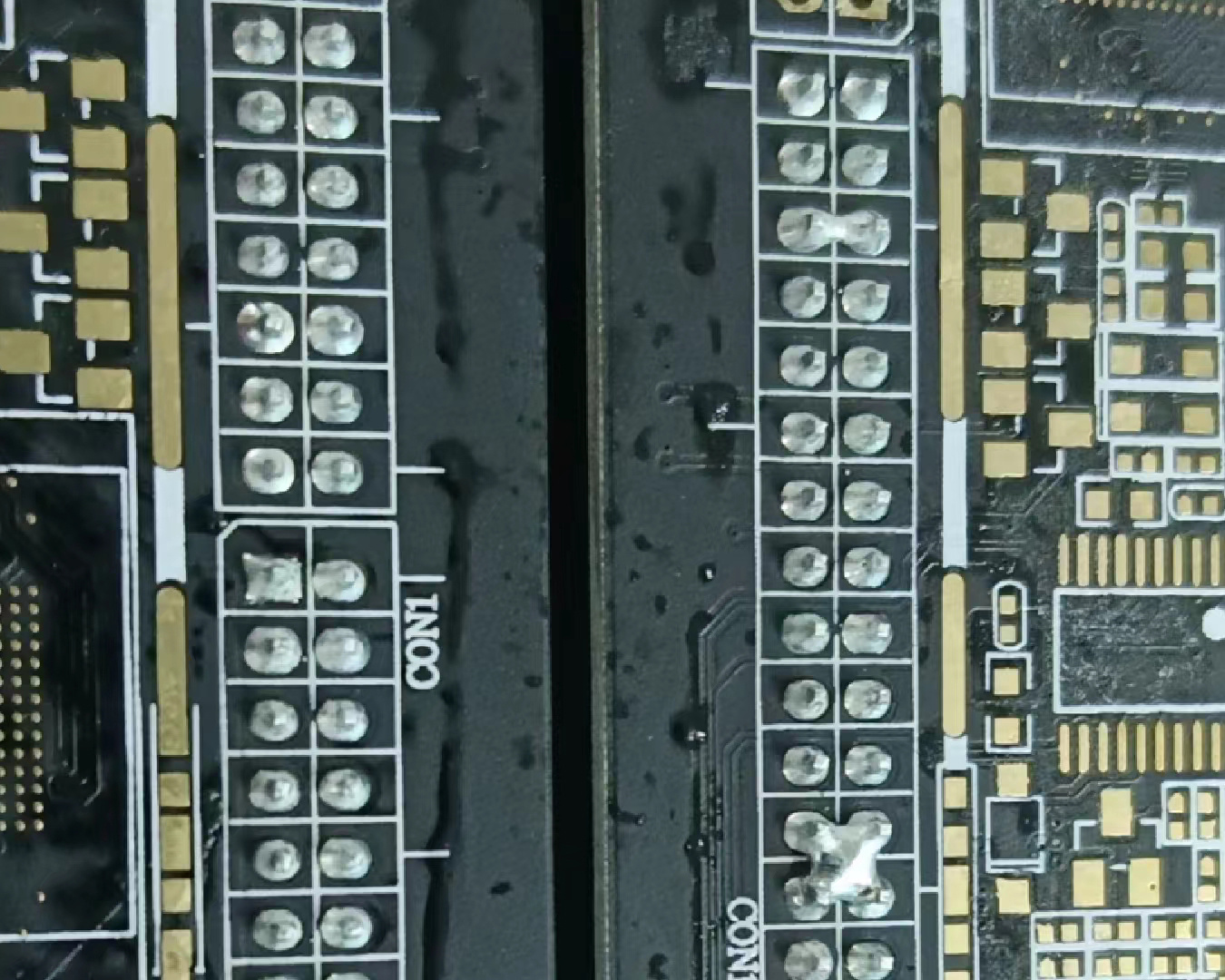
The reasons for selective wave soldering tin connection may include
作者:
Selective Wave Soldering
2023-11-14 13:41
1. If the preheating temperature is too low, it will lead to poor activation of the flux and insufficient temperature of the PCB board, resulting in poor wetting power and fluidity of the liquid solder, and bridging of solder joints between adjacent circuits.
2. The surface of the PCB board is not clean, which affects the fluidity of liquid solder on the PCB surface. The solder is easily blocked between solder joints, forming a bridge.
3. If the solder is impure and contains impurities exceeding the allowable standards, the characteristics of the solder will change, and the wetting or fluidity will gradually deteriorate.
4. Poor soldering flux that cannot clean the PCB reduces the wetting force of the solder on the surface of the copper foil, resulting in poor wetting.
5. The PCB board is deeply immersed in tin, the soldering flux is completely decomposed or not smooth, and the solder joints are not desoldered in a good state.
6. The component pins are too long, resulting in adjacent solder joints not being able to "single" remove tin when they break away from the solder wave peak. Alternatively, if the long pins are soaked in tin temperature for too long, the flux on the surface of the pins will be coking, and the fluidity of the solder between the pins will decrease, resulting in the possibility of bridge formation.
7. If the welding angle is too large, the probability of coplanar and bridging between the front and rear solder joints when they detach from the wave peak is smaller.
8. When the component density is high, the design of the solder pad shape is poor, or the welding direction of the insertion and IC components is incorrect.
9. PCB board deformation can cause inconsistent depth of pressure waves in the left, middle, and right parts of the PCB, and result in poor tin flow in areas with deep tin, which is prone to bridging.
Related News
Building B, Lin Po Hang Sha Tou Industrial Zone, National Road 107, Shangliao Community, Xinqiao Street, Baoan , Shenzhen

Follow us
Links:
© 2022 AST (SHENZHEN) INTELLIGENT TECHNOLOGY CO., LTD. 粵ICP备********号 SEO


